Chapter 3: Digital Logic Structures
Transistors, Circuits, and Logic Gates.
The Transistor #
Transistors are semiconductor devices that can amplify or toggle (switch) electrical signals and are the basic units in any modern Computing System.
There are two types of transistors that are commonly in used:
- Bipolar Junction Transistor (BJT)
- Field-Effect Transistor (FET)
Some of their main differences are:
| BJT | FET |
|---|---|
| Electrical current is controlled with current. | Electrical current is controlled with voltage. |
| Affected by temperature quickly. | Affected by temperature less. |
| Breaks quickly. | Durable. |
| Suitable for hobby electronic devices. | Suitable for commercial products. |
| Low switching speed. | High switching speed. |
In both cases these transistors have three terminals that have the same characteristics:
| BJT | FET | Terminal Description |
|---|---|---|
| Base | Gate | Control terminal; controls the current of electrical signal. |
| Emitter | Source | Input terminal; supplies the transistor with electrical current. |
| Collector | Drain | Output terminal; the electrical current going out of the transistor. |
Both transistors also contain N-Type or P-Type semiconductors that changes the behaviour of the current flowing to the transistor based on the configuration:
| BJT | FET | Current Flow Description |
|---|---|---|
| NPN | N-Channel | Current flows from the output terminal to the input terminal |
| PNP | P-Channel | Current flows from the input terminal to the output terminal |

In general, N-Type and P-Type transistors are complimentary of each other:
- N-Type transistors allows the flow of electrical current if voltage is given.
- P-Type transistors stops the flow of electrical current if voltage is given.
A common circuit design that takes advantage of these properties of transistors is called the CMOS (Complimentary Metal-Oxide Semiconductor) circuit and is the basis for most Logic Gates.
Logic Gates #
Logical operators built from transistors; digital logic circuits.
The ff. are schematic symbols of digital logical operators:

Combinational Logic Circuits #
A combinational (or combinatorial) logic circuit is a type of digital logic whose operations are pure ie. it doesn't have state or use memory and only generates outputs based from its inputs.
Decoder #
A decoder is a combinational logic circuit that contains outputs where is the number of inputs.
Each output terminal in a decoder corresponds to the bit permutation of the input terminals.

Decoder truth table:
| a | b | s0 | s1 | s2 | s3 |
|---|---|---|---|---|---|
Multiplexer (Mux) #
A multiplexer (or mux) is a combinational logic circuit that contains inputs, select terminals, and output terminal.
A multiplexer's output is determined by the permutation of the select signals from given input signals.

Multiplexer truth table:
| s0 | C |
|---|---|
Here, whenever is the output of the multiplexer is whatever value has, and whenever is the output of the multiplexer is whatever value has.
Conversely there is also the demultiplexer which contains a single input, outputs, and select terminals.
Full-Adder #
A full-adder (or 1-bit adder) is a combinational logic circuit that contains:
- Three (3) input terminals: two (2) of which are the operands for the sum operation and the other is the carry bit.
- Two (2) output terminals: one (1) for the carry-over bit and the other the sum bit.

Full-adder truth table:
There is also the notion of a half-adder which is essentially a full-adder but without a carry input terminal.
Basic Storage Elements #
The ff. are digital logic structures that can store/persist values which are building blocks for memory devices.
SR Latch #
The SR (set/reset) Latch is a digital logic structure that persists a single bit of information.
One of the most common way to implement SR Latches in a digital circuit is to use two (2) NAND gates whose output of each is one of the inputs of the other.

In an SR Latch, the or set input sets the state of the latch (in this case the output ) to a , whereas the or reset input resets or clears the state of the latch to a .
Assuming that the initial state of a circuit like this is the ff.:
In this case:
- will remain with a value of regardless of what the value of is iff. is .
- will remain with a value of regardless of what the value of is iff. is .
To build a basic intuition about how this works we can imagine an OR gate whose output feeds into one of its input:

Recall that the truth table of the OR logical operator is as follows:
For the OR gate in this case: if the input terminal is given a high input signal (a value of 1), then the output will equal to as which consequently will set .
Once at this state, will always be regardless of the value of .
NOTE: Please see Ben Eater: SR Latch for a video demonstration of this and a more indepth discussion on the SR Latch.
D-Latch #
The D-Latch (or Data Latch) is a digital logic structure that is an extension of the SR Latch.
The D-Latch uses a single input to toggle the state of the SR latch with an auxiliary input called the write-enable (WE) input.
The D-Latch can only change the state of the latch if the WE input is on.

NOTE: Please see Ben Eater: D-Latch on youtube for more information about the D-Latch digital logic circuit.
The Concept of Memory #
Computer memory is made up of (a large) number of locations that are each uniquely identifiable and can store a number of bits of information.
Address Cell, Address, and Addressability #
An address cell is a single unit or item within a memory device.
A memory address or just address is a location of an address cell in the memory.
The address size or addressability of a memory is the number of bits of information that can be stored in an address cell.
So for example, a computer that is advertised to have 2 GB of memory may mean that it has 2 billion addresses to uniquely identify each cell where each can store a byte of information.
Address Space #
The address space refers to the total number of addresses that can uniquely identify an address cell in a memory device.
Given bits, we can uniquely identify address cells ie. bits can be used to uniquely identify address cells.
Addressability #
As mentioned earlier, addressability refers to the number of bits that can be stored in each memory address.
A byte-addressable memory is a device that contains 8-bits or a byte in each address cell.
A word-addressable memory is a device that contains the same word-length as the CPU in each address cell.
A word is a size that is dependent on each CPU design/implementation.
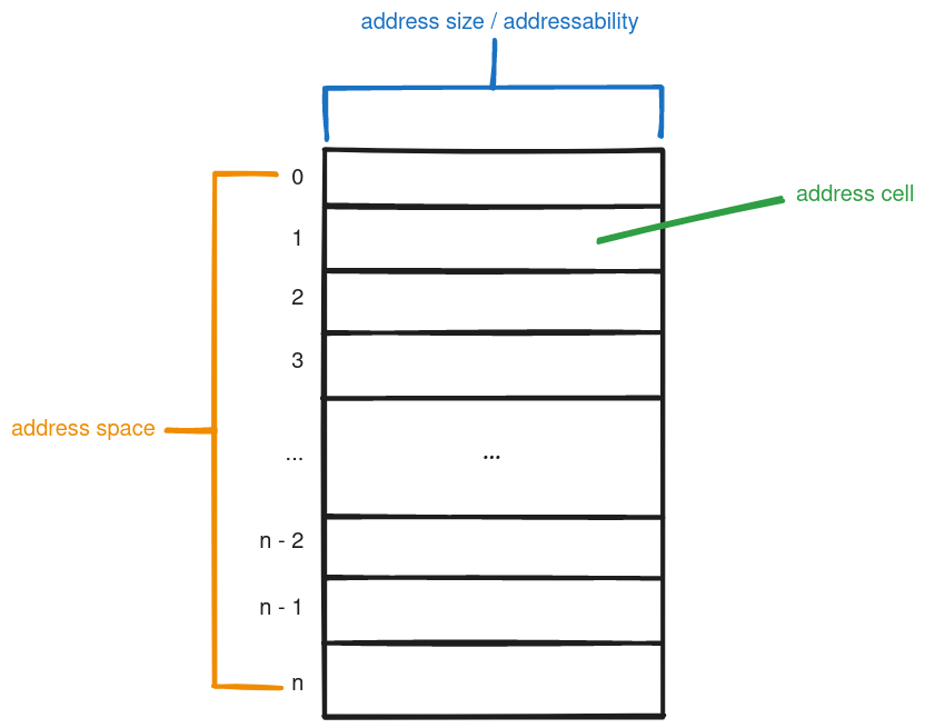
A Memory Diagram #
The ff. is a memory diagram depicting the different parts of an abstract memory device.
The diagram contains sections for the address cell, an -length address space, and the address size or addressability of each address cell.